Introduction to Thermal Copper Pillar Bump Technology
Definition: What is a Thermal Copper Pillar Bump?
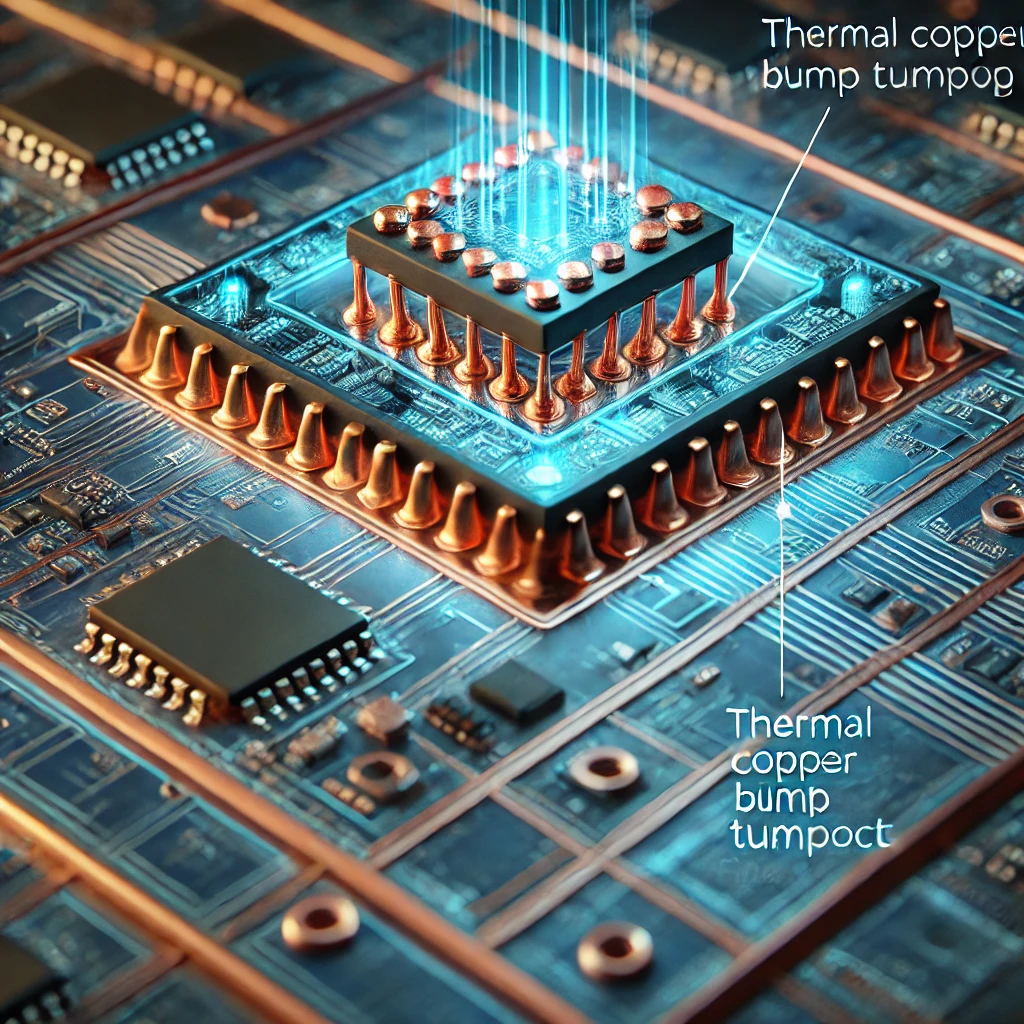
A thermal copper pillar bump is a high-performance interconnect technology used in advanced semiconductor packaging. Unlike traditional solder bumps, copper pillars provide better thermal and electrical performance, making them ideal for high-speed, high-density applications such as flip chip bonding and 3D IC packaging. The structure typically consists of a copper column with a solder cap, ensuring superior mechanical reliability and efficient heat dissipation.
Evolution: From Solder Bumps to Copper Pillar Technology
The semiconductor industry has evolved from wire bonding and traditional solder bumps to copper pillar bumping, driven by the need for finer pitch interconnects and better thermal management. Compared to older lead-based solder bumps, copper pillar bumps:
- Enable higher density by reducing the pitch between bumps.
- Improve thermal performance due to copper’s superior heat dissipation.
- Enhance mechanical stability with increased electromigration resistance.
Major semiconductor manufacturers, including Intel, TSMC, and AMD, have adopted copper pillar technology for next-generation processors, GPUs, and high-performance computing (HPC) chips.
Importance of Copper Pillars in Flip Chip Bonding & 3D IC Packaging
Advanced packaging pillars play a critical role in flip chip bonding, where the chip is mounted face-down onto a substrate using bumps for electrical connections. Key benefits include:
- Lower resistance & improved signal integrity for high-speed applications.
- Reduced form factor, enabling compact smartphones, wearables, and IoT devices.
- Better heat dissipation, preventing overheating in AI, 5G, and data center processors.
In 3D IC packaging, copper pillars are essential for vertical stacking of multiple silicon dies, ensuring efficient power delivery and thermal management. This makes them crucial for HPC, AI accelerators, and next-gen semiconductor devices.
With the growing demand for miniaturized, high-performance electronics, thermal copper pillar bump technology is becoming the industry standard for high-reliability, high-speed interconnects.
How Copper Pillar Bumps Work
Structure & Composition of Copper Pillar Bumps
Copper pillar bumps are multi-layered structures designed for high-performance semiconductor packaging. They consist of:
- Copper Core: The main structural component, offering low resistance, high thermal conductivity, and superior electromigration resistance.
- Barrier Layers (Nickel/Titanium): Prevents the diffusion of copper into the solder while enhancing mechanical strength.
- Solder Cap (SnAg or SnPb Alloy): Ensures reliable bonding with the substrate and allows for controlled reflow during flip chip bonding.
Unlike traditional solder bumps, copper pillars allow for finer pitch interconnects, reducing the overall package size while enhancing electrical and thermal performance.
Fabrication Process: Step-by-Step Breakdown
The copper pillar bumping process involves multiple precision-driven steps to ensure optimized interconnect performance:
- Photolithography: A mask defines the regions where the copper pillars will be electroplated.
- Copper Electroplating: Copper is deposited onto the wafer to form the pillar structure, ensuring high conductivity and durability.
- Barrier Metal Deposition: A nickel, titanium, or palladium layer is added to prevent copper diffusion and strengthen the interconnect.
- Solder Cap Application: A lead-free solder cap is placed on top of the copper pillar for flip chip bonding compatibility.
- Reflow Process: The wafer undergoes controlled heating, allowing the solder to flow and form strong electrical connections.
- Etching & Final Processing: Unwanted material is removed, and the wafer is prepared for dicing and integration into advanced IC packaging.
Copper Pillar vs. Traditional Solder Bumps: Why Copper Wins
Copper interconnects offer significant advantages over conventional solder bumps:
| Feature | Copper Pillar Bumps | Traditional Solder Bumps |
|---|---|---|
| Thermal Performance | Superior heat dissipation due to copper’s high conductivity. | Lower thermal efficiency, leading to overheating risks. |
| Mechanical Strength | Higher durability and resistance to fatigue. | Prone to cracking under thermal cycling. |
| Electromigration Resistance | Enhanced resistance, making it ideal for high-current applications. | Weaker under prolonged high-power conditions. |
| Fine Pitch Capability | Supports advanced packaging with smaller interconnect spacing. | Limited miniaturization, restricting high-density chip designs. |
With growing demand for high-speed computing, AI processors, and 5G technology, copper pillar bumps have become the industry standard for flip chip bonding and next-gen semiconductor devices.
Advantages of Using Copper Pillars in Flip Chip Bonding
Copper pillar bump technology has become a crucial advancement in flip chip bonding, offering significant benefits over traditional solder bumping. Below are the primary advantages of using copper pillars:
Improved Electrical Conductivity
Copper interconnects provide superior electrical performance compared to traditional solder bumps. The high conductivity of copper enhances signal integrity, making it ideal for high-frequency applications such as advanced microprocessors and RF devices. Additionally, the lower electrical resistance reduces power losses, improving overall energy efficiency.
Better Thermal Management
One of the key benefits of thermal copper pillar bumps is their enhanced heat dissipation capabilities. Copper has excellent thermal conductivity, which allows for efficient heat spreading, reducing the risk of overheating in power-intensive semiconductor devices. This is particularly important for high-performance computing (HPC) chips, GPUs, and AI accelerators.
Miniaturization & High-Density Interconnects
Copper pillars enable finer pitch interconnections, allowing for increased I/O density in semiconductor packaging. This is essential for the latest-generation processors and 3D IC packaging, where space constraints demand compact yet highly efficient interconnects. Compared to solder bumps, copper pillars facilitate the scaling of semiconductor devices while maintaining reliable electrical and thermal performance.
Reliability & Durability
Copper pillars exhibit greater mechanical strength and improved resistance to electromigration, which enhances the longevity of semiconductor devices. Unlike solder bumps, which can suffer from fatigue and cracking over time, copper pillars maintain structural integrity under thermal and mechanical stress. This makes them a more durable interconnect solution, reducing failure rates in electronic devices.
The adoption of copper pillar technology in flip chip bonding has revolutionized semiconductor packaging. With superior electrical and thermal properties, improved reliability, and the ability to support high-density interconnects, copper pillars have become essential for next-generation semiconductor designs. As packaging technologies evolve, copper pillar bumps will continue to play a pivotal role in enabling high-performance, energy-efficient, and durable electronic devices.
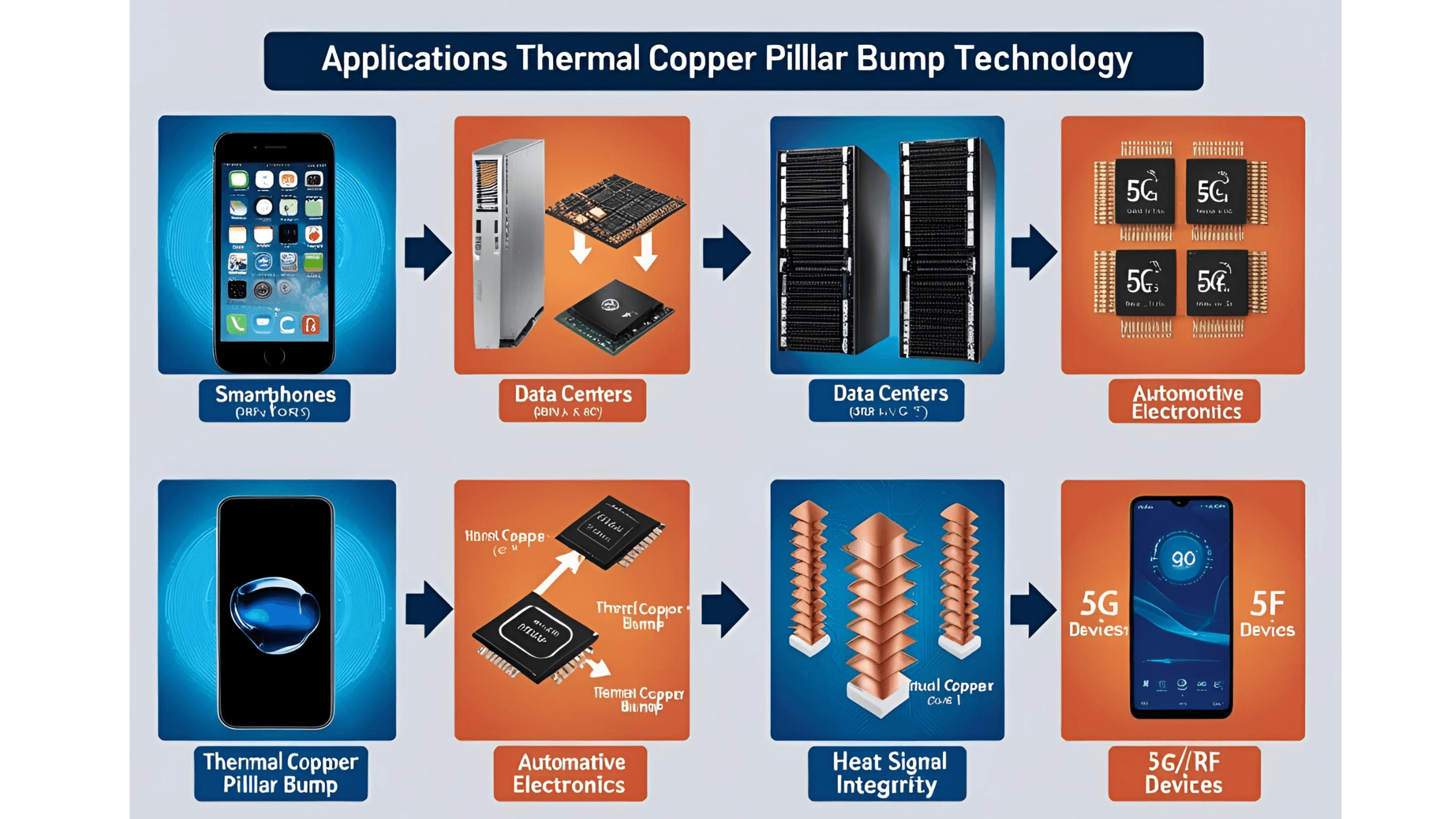
Applications of Thermal Copper Pillar Bump Technology
- Smartphones & Consumer Electronics
Copper pillar bump technology plays a critical role in modern mobile and consumer electronics. It enables high-performance processors and system-on-chips (SoCs) in smartphones, tablets, and laptops by providing better electrical conductivity and heat dissipation. With shrinking semiconductor nodes and increasing transistor densities, copper pillars support the finer pitch requirements of advanced microprocessors and memory chips. - Data Centers & AI Chips
AI accelerators, GPUs, and high-speed networking chips used in data centers require high-density interconnects with superior thermal performance. Copper pillar bumps are essential in packaging these components, as they reduce electromigration issues and enhance power delivery, ensuring reliability under heavy workloads. - Automotive Electronics
The automotive industry is increasingly reliant on semiconductor advancements, particularly in advanced driver assistance systems (ADAS), infotainment, and autonomous vehicle technologies. Copper pillar-based flip chip bonding ensures the durability and performance required for these applications, where extreme temperature variations and high-reliability standards are essential. - 5G & RF Devices
The expansion of 5G networks and high-frequency RF devices demands low-loss, high-speed interconnections. Copper pillar bumps, with their improved signal integrity and resistance to electromigration, are crucial for fabricating 5G base stations, millimeter-wave antennas, and RF front-end modules.
Challenges in Implementing Copper Pillar Bumps
- Manufacturing Complexity
The fabrication of copper pillar bumps requires precision electroplating and advanced lithography techniques to achieve fine pitches below 40µm. This complexity increases production costs and demands cutting-edge semiconductor manufacturing capabilities. - Material Compatibility
Low-K dielectric materials used in ultra-thin interconnect layers can pose challenges in reliability and mechanical stability. Copper pillars must be carefully integrated to avoid delamination and stress-related failures. - Thermal & Mechanical Stress
Managing thermal expansion mismatch between Advanced packaging pillars and silicon chips is crucial to prevent cracks and reliability issues. The higher stiffness of copper compared to traditional solder bumps can introduce additional mechanical stress during thermal cycling. - Cost Considerations
Although copper pillar technology offers long-term reliability advantages, the initial investment in new lithography and plating processes can be high. Manufacturers must weigh the benefits of performance gains against the added cost of upgrading fabrication facilities.
Future Trends in Copper Pillar Bump Technology
- Integration with 3D IC Packaging
Copper pillar bumps are a fundamental enabler of advanced 2.5D and 3D IC packaging. These interconnects allow for chip stacking and heterogeneous integration, reducing power consumption and improving data transfer speeds in multi-chip modules. - Advanced Solder-Free Designs
New interconnect techniques, such as direct copper-to-copper hybrid bonding, are emerging to replace solder-based connections. This advancement enhances reliability by eliminating solder fatigue and improving thermal conductivity. - Nanomaterial Innovations
Researchers are exploring graphene-enhanced solder layers and other nanomaterials to further improve electromigration resistance and extend the lifespan of copper pillar interconnects. - Industry Adoption
Leading semiconductor manufacturers, including Intel, TSMC, and Samsung, are driving the adoption of copper pillar technology in next-generation processors, AI accelerators, and high-performance computing chips. This trend is expected to accelerate as packaging demands continue to evolve.
By overcoming current manufacturing challenges and leveraging future innovations, thermal copper pillar bump technology is set to play a crucial role in the future of high-performance microelectronics and semiconductor packaging.
Conclusion: The Future of Thermal Copper Pillar Bump Technology
Thermal copper pillar bump technology has emerged as a key innovation in semiconductor packaging, driving advancements in flip chip bonding, microelectronic packaging, and high-density interconnects. By offering superior electrical conductivity, enhanced thermal management, and greater reliability, copper pillars have revolutionized smartphones, AI accelerators, automotive electronics, and 5G infrastructure.
Despite the benefits, challenges such as manufacturing complexity, material compatibility, and cost considerations continue to impact widespread adoption. However, the industry is rapidly evolving, with 3D IC packaging, hybrid bonding, and nanomaterial innovations paving the way for next-generation semiconductor designs.
As major industry players like Intel, TSMC, and Samsung invest in copper pillar bump technology, its role in enabling high-performance computing, artificial intelligence, and advanced communications will only grow. This technology is not just a milestone in semiconductor packaging—it is shaping the future of microelectronics, ensuring higher efficiency, miniaturization, and durability in tomorrow’s devices.
Explore More Cutting-Edge Technologies
If you’re interested in how next-generation computing and storage technologies are evolving, check out these in-depth articles:
🔹 Memristors: Evolution, Applications, and Neuromorphic Computing – Learn how memristors are shaping the future of AI-driven computing by mimicking brain synapses.
🔹 Optical Computing: The Next Leap in High-Speed Processing – Discover how light-based computing could revolutionize data processing speeds beyond traditional silicon chips.
🔹 Magnonics: The Future of Spin-Wave Computing – A deep dive into how magnonics is enabling ultra-fast, energy-efficient computing beyond semiconductor limitations.
🔹 The Rise and Fall of Bubble Memory in Computer Storage – A fascinating look at bubble memory technology, its historical significance, and why it faded into obscurity.